 Fraunhofer Group for Microelectronics
Design for Smart Systems
ESD: New measuring technologies offer effective protection
Microelectronic devices and systems are getting smaller and more complex – this also presents ESD protection with new challenges. Many established test methods are reaching their limitations. Researchers at Fraunhofer EMFT have developed new solutions that provide more accurate and reproducible measurement results.

We have all experienced it: you touch a doorknob and suddenly get a shock because you just walked across a carpet. This is the fault of electrostatic discharges (ESD), which result from an imbalance in positive and negative charge between two objects. Around 3000 V are required before a human can feel a discharge of this type. Semiconductor modules are not quite as sturdy: as little as 30 V can result in damage or functional impairment to such devices. Often, only certain parameters are shifted, which can lead to higher power consumption, for example. This can, however, reduce the service life of a battery, rechargeable or otherwise.
The leeway involved is getting smaller and smaller
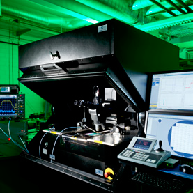
The continuing trend for miniaturization in microelectronics is another factor contributing to new challenges: the increasingly delicate structures of the devices also reduce the maximum permissible discharge voltage. Today’s conventional test methods are hitting their limits more and more as they are often incapable of mapping reality. With the oft-used CDM (Charged Device Model), where a device is charged and then discharged, difficult to control air discharges are, for example, often the result. This leads to fluctuating measurement results and low levels of reproducibility. For the narrow ESD tolerance range of miniaturized devices, however, absolutely exact measurements are indispensable. Researchers at the Fraunhofer Research Institution for Microsystems and Solid State Technologies EMFT have, in Capacitive Coupled Transmission Line Pulsing (CC-TLP), developed and patented a measurement technology that allows for CDM levels of load with much greater precision and reducibility. The device is first contacted, and then the pulse is triggered. An additional benefit of CC-TLP is that testing can already be carried out on wafers, meaning that weaknesses from an ESD point of view can be detected early.
Design-related disruptive effects play an important role
The demands placed on test methods at the system level are even more complex, as currents may arise within the system that cannot be predicted within the simulation model. The Munich-based experts have therefore come up with an expanded measuring process with an integrated current sensor. “In one case, this approach showed us that secondary discharge was occurring in an air gap between the base plate of the measuring station and a metal cap on the system housing. Our measurements demonstrated that there were very strong currents of around 600 A for a brief period,” explains group leader Dr. Horst Gieser. Phenomena such as this, which are often design-related, occur relatively often and cannot be controlled. This makes it even more important to include these disruptive effects in the analyses in order to develop more effective protective concepts. In the case previously described, the researchers identified four sensitive lines and integrated resistors at the critical pins. This allowed all disruptive influences to be eliminated systematically, increasing the robustness of the system.
Last modified: