 Fraunhofer Group for Microelectronics
Measurements in the nanometer range – a quantum sensor made of diamond finds even the smallest defects
Integrated circuits in electronics are becoming more and more complex, and the structures on them are getting ever smaller. In modern hard disks, the individual magnetic bits – the zeros and ones – are only 10 – 20 nm in size. Tiny magnetic fields need to be measured in order to detect the current flow through electronic circuits or to find defective segments of the hard disk. This is now possible thanks to a new quantum sensor made of diamond, which is being developed by Fraunhofer IAF in conjunction with the Max Planck Institute for Solid State Research.
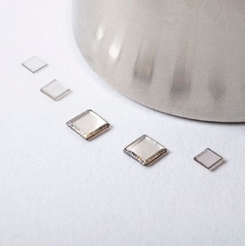
The sensor itself is nanoscale: its tip is made of synthetic diamond. Five nanometers below the surface of this diamond, a carbon atom is replaced with a nitrogen atom. Directly beside it, there is a carbon gap, and its potential traps an electron. The magnetic moment (spin) of this single electron can be oriented, which allows it to function as the smallest possible “sensing magnet” in the tip of the diamond. It reacts to external magnetic fields such as those found on hard disks and in the conductor paths of electronic circuits.
Artificial production of diamonds has been continuously developed and optimized at the Fraunhofer Institute for Applied Solid State Physics IAF over the last few decades. In microwave plasma reactors, the crystals are synthesized from the carbon atoms contained in methane by adding hydrogen. In the reactor, the diamond layers grow on special substrates that are separated using a laser and are then polished. Their planned deployment in quantum sensors places particular demands on the crystals: all starting materials must be pre-cleaned in order to guarantee that the diamond layers are ultra-clean. The methane used to manufacture the diamond sensor must be isotopically pure to ensure that only the electron in the tip of the diamond has a magnetic moment.
Conductor paths and hard disks can be examined in detail
The sensor is intended to precisely determine both the position and strength of even the smallest magnetic fields. Optically detected electron spin resonance spectroscopy makes this possible. Using this process, the nitrogen vacancy center in the diamond is irradiated with laser light while “feeling” the locations to be inspected. The sensor is thus excited into emitting its own light. The characteristic properties of the backscattered light allow conclusions to be drawn about the position and strength of the magnetic field being measured.
The sensitive sensor can detect magnetic fields of individual electrons and atomic nuclei in structures that are only a few nanometers in size. In the case of an electronic circuit, the quantum sensor can be used to test the functionality of conductor paths, for example. One other important area of application of the quantum sensor is the quality control of hard disks. This measuring method can be used to quickly and precisely identify defective data segments; these segments can then be skipped during disk reading and writing. This significantly reduces the reject rate and thus also the production costs for future hard disks.
Last modified: