 Fraunhofer Group for Microelectronics
New material to push the boundaries of silicon-based electronics
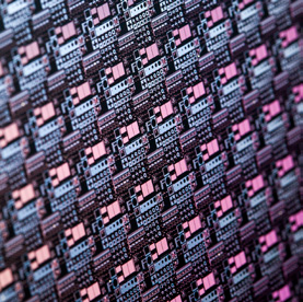
Scandium aluminum nitride (ScAlN), a semiconductor material that has so far been little researched in microelectronics, is being used in the recently launched project “Power Electronics 2020+”. The aim is to develop more efficient power electronic systems and to pave the way for the next generation of electronics. This is because electronics based on silicon (Si), which has so far dominated the market, will no longer be able to meet increasing industrial demands in the foreseeable future.
Limits of silicon technology
Silicon, a low-cost semiconductor material with an almost perfect crystalline structure, is beginning to hit its physical limits: power electronic components made of Si are inadequate, especially with regard to the required power density and compactness.
New material composition for more power and efficiency
The use of the semiconductor gallium nitride (GaN) in power electronics has already overcome the limitations of Si technology. At very high voltages, temperatures, and switching frequencies, GaN offers better performance than Si and thus enables significantly higher energy efficiency. In the project “Research into Functional Semiconductor Structures for Energy-Efficient Power Electronics”– or “Power Electronics 2020+” for short – researchers are working on further increasing the energy efficiency and service life of future electronic systems. To this end, another material is to be used for the first time: ScAlN.
First ScAIN-based devices
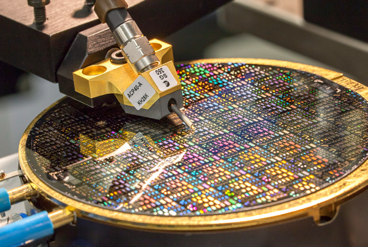
ScAlN is very promising as a piezoelectronic semiconductor material because its physical properties make it particularly suitable for use in power electronic components. Specifically, the aim is to grow ScAlN on a GaN layer, adapted to the lattice, and to process transistors with high current carrying capacity with the heterostructures produced from it.
“The components achieve a higher power density measured on the chip surface as well as higher switching speeds and higher operating temperatures, which amounts to lower switching losses, higher energy efficiency, and more compact systems,” explains Prof. Oliver Ambacher, Director of the Fraunhofer Institute for Applied Solid State Physics IAF.
Pioneering work in materials research
One of the biggest challenges of this project is crystal growth, as neither growth recipes nor empirical values exist for this material structure. The project team will have to jump this hurdle in the coming months in order to achieve reproducible results and produce layer structures that can be successfully used for power electronic applications.
Project participants:
• University of Freiburg
• Fraunhofer IAF
• Fraunhofer IIS
• Leistungszentrum Elektroniksysteme
• Sustainability Center Freiburg
Last modified: