 Fraunhofer Group for Microelectronics
Ceramic embedding for the power electronics of the future
The trend towards miniaturization and three-dimensional integration is pushing power devices to their limits, particularly with regard to temperature resistance and high switching speeds, while also maintaining a long service life. The applicability of established setup concepts based on PCBs (printed circuit boards) and LTCC (low-temperature co-fired ceramic) is limited here. This is where an innovative setup concept comes in, based on embedding of devices in a ceramic circuit carrier.
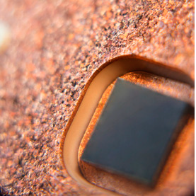
In this technology, which is known as DCB (direct copper bonded) embedding, the power semiconductors are integrated into specially prepared DCB substrates using suitable packaging and are then enclosed in a grout. The DCB substrate is prepared using laser structuring. The considerable copper layer thicknesses result in a high current-carrying capacity. Various ceramic materials can be used for insulation. A suitable material is selected by considering the optimization of high-temperature resistance, heat management, and mechanical properties. The electrical connections are formed by means of integrated vias (through-plating). The use of additional vias allows the manufacture of multi-layer DCB stacks, which are of particular benefit in low-inductance applications. Development of DCB embedding technology at Fraunhofer IISB will continue intensively over the years to come in order to fully exploit the potential offered by wide-band-gap devices for use in power-electronic applications.
Last modified: