Smart and Healthy Living
Quadruple data rate thanks to 3D integration
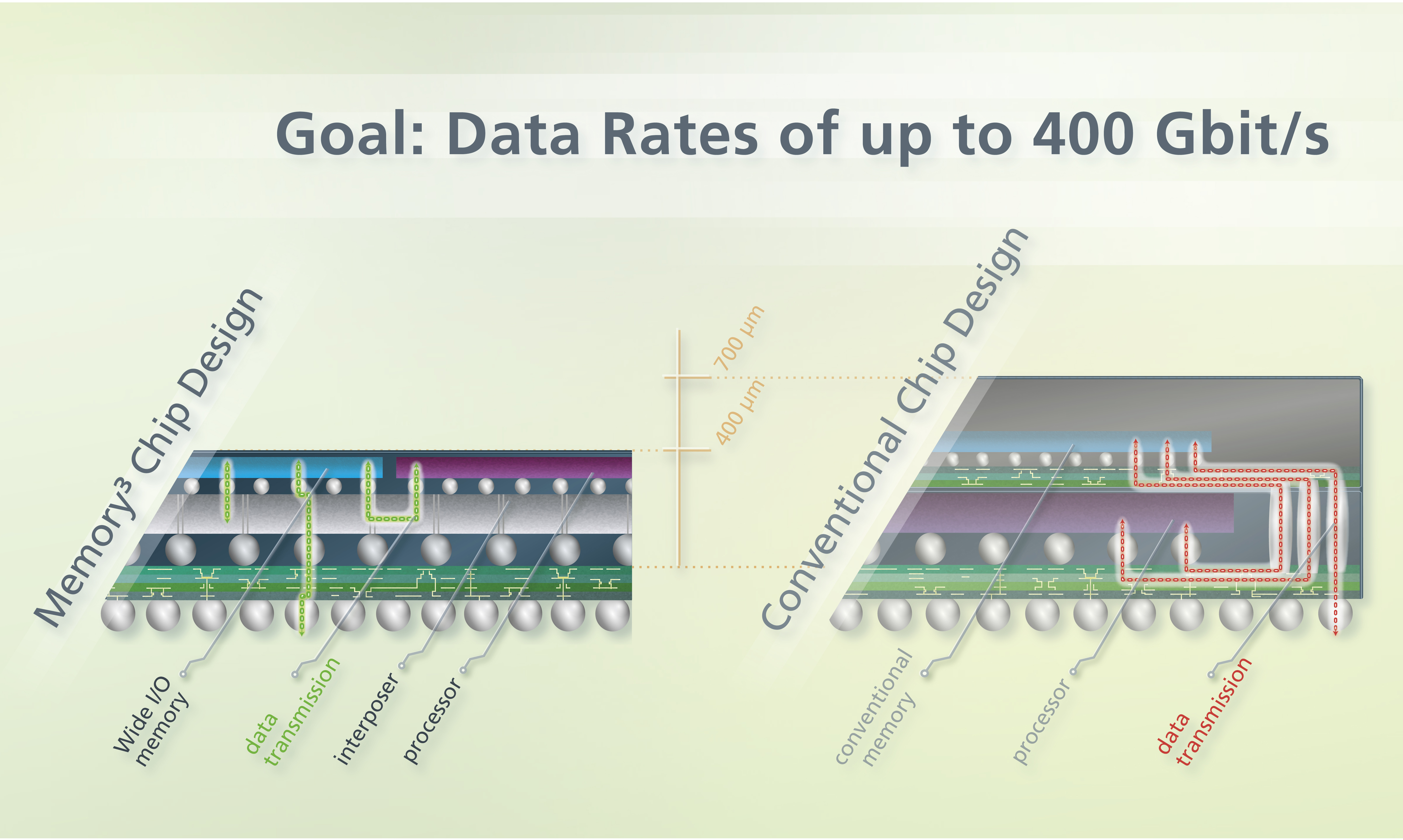
Small is beautiful – and that applies to microchips too. We have reached the stage, however, where classic structures with standardized device sizes are pushing at their limits. One example is the electronics in ultra HD cameras, which can capture four times as many pixels as cameras with full HD. In order to be able to process the quantities of data produced in an energysaving manner and in a small space, the arrangement of the processor and the wide I/O memory on the circuit board was rethought three dimensionally. This idea was put into practice by researchers from Fraunhofer IIS’ division EAS. For the “Memory³” project, they developed a chip structure that can satisfy the high-performance requirements of ultra HD cameras.
The “trick” behind the new chip is to reduce the line width: the processor and memory are arranged in the same housing. Between them, a thin substrate (known as an interposer) functions as a data line. This superfine line structure allows the processor and the memory to “merge” so closely that data exchange is considerably accelerated. The data can be transmitted at a speed of up to 400 GBit/s – four times what has previously been possible. Another advantage is that energy consumption drops. The experts needed around a year and a half for theoretical development and construction of a prototype.
The development partner, Dream Chip Technologies, supported the team particularly in the area of applications. The current structure of the 3D microchip was developed with special consideration for ultra HD cameras. It could, however, be used in the future in other areas such as graphic cards or switching nodes for fiberglass networks.
The Memory³ project was supported by Germany Federal Ministry for Economic Affairs and Energy as part of the Central Innovation Program SME.
Last modified:
