 Fraunhofer Group for Microelectronics
Semiconductor based Technologies
Leading edge equipment for 5 nm technology
The continuing rapid development in the semiconductor industry also places special demands on the processes for structure transfer to silicon wafers – lithography. The state of the art in the most advanced semiconductor companies is currently the realization of a structure width below 10 nm. This is to be further reduced to increase packing density, energy efficiency and the switching speed of the components. Considerations of economic efficiency also promote this trend.
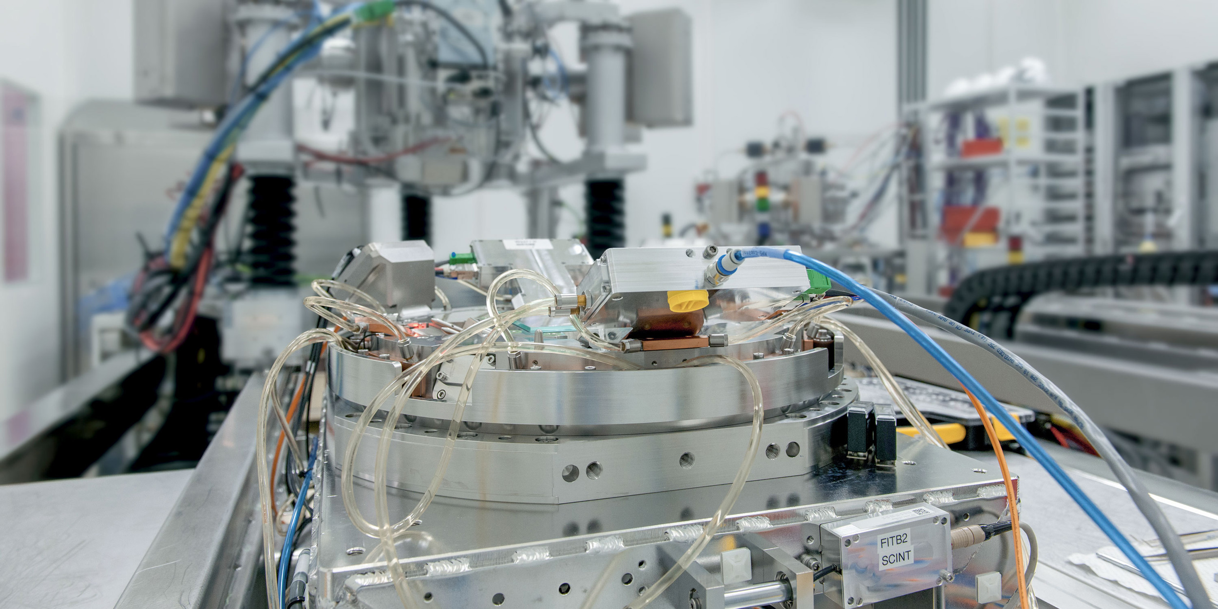
Fraunhofer ISIT and the company IMS Nanofabrication GmbH have been developing innovative processes for several years, with which silicon wafers can be processed using complex microsystems technology. The final product of this processing is the core of the multi-beam mask writer developed by IMS Nanofabrication. It supports the implementation of an electron multi-beam writing process, which enables the production of masks of highest resolution. By processing at Fraunhofer ISIT, a microchip developed by IMS Nanofabrication allows 262,000 individually addressable electron beams to be switched on and off and thus used for mask structuring. For each of these electron beams, an opening with a shielded gold control electrode is realized on this microchip at the institute. Fraunhofer ISIT uses highly developed microsystem techniques for the necessary processes for structuring.
As a result of this successful cooperation, the next milestone in semiconductor manufacturing technology will be reached: the production of leading-edge 5 nm chips. These have been in production at leading semiconductor manufacturers since the first half of 2020, using the IMS multi-beam mask writer to produce masks for EUV lithography (with 13.5 nm light wavelength) on silicon wafers.
The project partner:
The Viennese company IMS Nanofabrication GmbH manufactures the mask writers. The production equipment is used for mask production. The Multi-Beam Mask Writing Technology (MBMW) is unique worldwide and a key to the production of nanoelectronic devices.
Last modified: