 Fraunhofer Group for Microelectronics
Thick aluminum for packaging
The Fraunhofer Institute for Electronic Nano Systems ENAS, in cooperation with several partners, has developed a process for the deposition of thick aluminum layers (Al layers) on circuit boards, silicon, and ceramic substrates. Electrochemical deposition from ionic Al allows the manufacture of layer thicknesses of over 1 μm. These layers can be used as a conducting path and as a bond pad for wire-bond contacts.
Why aluminum?
Over the last few years, aluminum (Al) as a material for electric wires has been replaced by copper (Cu) in many areas of everyday life. The electrical and heat conductivity of Al is lower than that of Cu, but Al’s ratio of density to conductivity is better. With Al, you need a 40 % thicker layer in order to be able to conduct the same quantity of electricity as with Cu, but the Al layer is 50 % lighter. One additional advantage is Al’s wire-bonding capability. This saves not only Cu, but also the typical nickel-gold or nickel-palladium-gold finishing metallizations. Al also maintains a stable price and offers better physical and machining properties. The aim is to reduce the use of copper and subsequent finishing metallizations in order to conserve valuable raw materials and to make circuit boards lighter.
Requirements of the process
The circuit board industry is dominated by medium-sized companies that need a smooth process. Galvanization, as a robust and established coating technology, is indispensable for circuit boards. That is why the Al coating also needs to be formed using a galvanic process. Aqueous solutions are unsuitable for Al deposition as Al has a more negative reduction potential than water and thus water decomposition would occur earlier. The idea for the procedure is based on the recognition that ionic liquids offer a way to deposit Al. The process has been described frequently in the literature over the last 20–25 years, but an application has yet to be found.
Process sequence and characterization
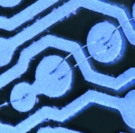
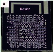
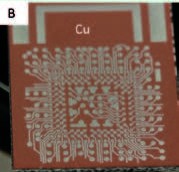
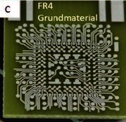
For the manufacture of conductor paths, a Cu-clad standard circuit board with a structured photoresist is used to begin with. In the open structures, Al is galvanically deposited on the Cu seed layer. The photoresist is then removed and the Cu is etched. Detached Al structures are left behind. The layer thicknesses are around 25 μm. Wire bonding is easily possible with both thin and thick wires with the Al layers.
Outlook
The deposition processes must now move to a higher level. We need to move away from samples that are only 2 × 5 cm² to realistic sizes such as a credit-card format of approximately 5 × 8,5 cm². In order to really remove Cu from circuit boards, Al cladding will be required. To make this a reality, further-processing methods need to be worked out. Vias of up to 200 μm in diameter have been demonstrated to be possible, but only with a Cu starting layer. This layer also needs to be replaced, e.g. with graphite or electrically conductive polymers. The next steps will then be to develop appropriate packaging in order to attain an Al circuit board flexibility comparable to existing Cu circuit boards.
Last modified: