 Fraunhofer Group for Microelectronics
Gallium nitride for a powerful 5G cellular network
The fifth-generation cellular network (5G) will enable data transmission between people, devices, and machines in real time. So far, no technology exists that allows for a reliable, fast and energy-efficient 5G network. In the EU project “5G GaN2”, 17 partners from research and industry join forces in order to develop technologies based on gallium nitride.

To date, primarily people communicate via the wireless radio network. In the cellular network of the fifth generation (5G), however, cars, devices, and production machines will also transmit data in real time. In the future, these high data rates will be covered by frequency bands in the millimeter-wave range (> 24 GHz). They provide a ten times higher bandwidth in comparison to currently available frequency bands (< 3 GHz). However, these new frequency ranges cannot be served efficiently with present mobile and antenna technology.
Increased energy efficiency using gallium nitride technology
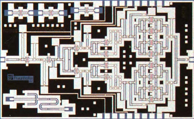
“It is crucial to improve the available output power and energy efficiency of the network infrastructure for these innovative frequency bands by using advanced gallium nitride technology,” says Dr. Dirk Schwantuschke, who manages the project on the part of the Fraunhofer Institute for Applied Solid State Physics IAF. In the 5G GaN2 project, components, devices, and circuits for the 5G base stations will be developed on the basis of gallium nitride (GaN).The contribution of Fraunhofer IAF to the overall project will be the development of power amplifiers in what is known as the E-band, the frequency range around 80 GHz.
Lowering costs and improving performance
Electronic devices and systems based on GaN are significantly more energy-efficient than conventional silicon (Si) ones. The GaN devices will optionally be applied on costefficient Si substrates. Another aspect of the project is the combination of various devices in a single package using innovative approaches with regard to packaging technologies, in order to reduce costs. The aim of the project is the realization of demonstrators at 28 GHz, 38 GHz, and 80 GHz. These demonstrators will serve as key technologies for the development of a powerful and energy-efficient 5G cellular network based on GaN.
The project reflects the entire value creation chain of cellular technology. Wafer suppliers, semiconductor manufacturers, and system integrators develop innovative GaNbased technologies for the cellular network of the fifth generation together with universities and research institutes.
Last modified: