 Fraunhofer Group for Microelectronics
Semiconductor based Technologies
Manufacturing technologies for 3 nm semiconductor technology
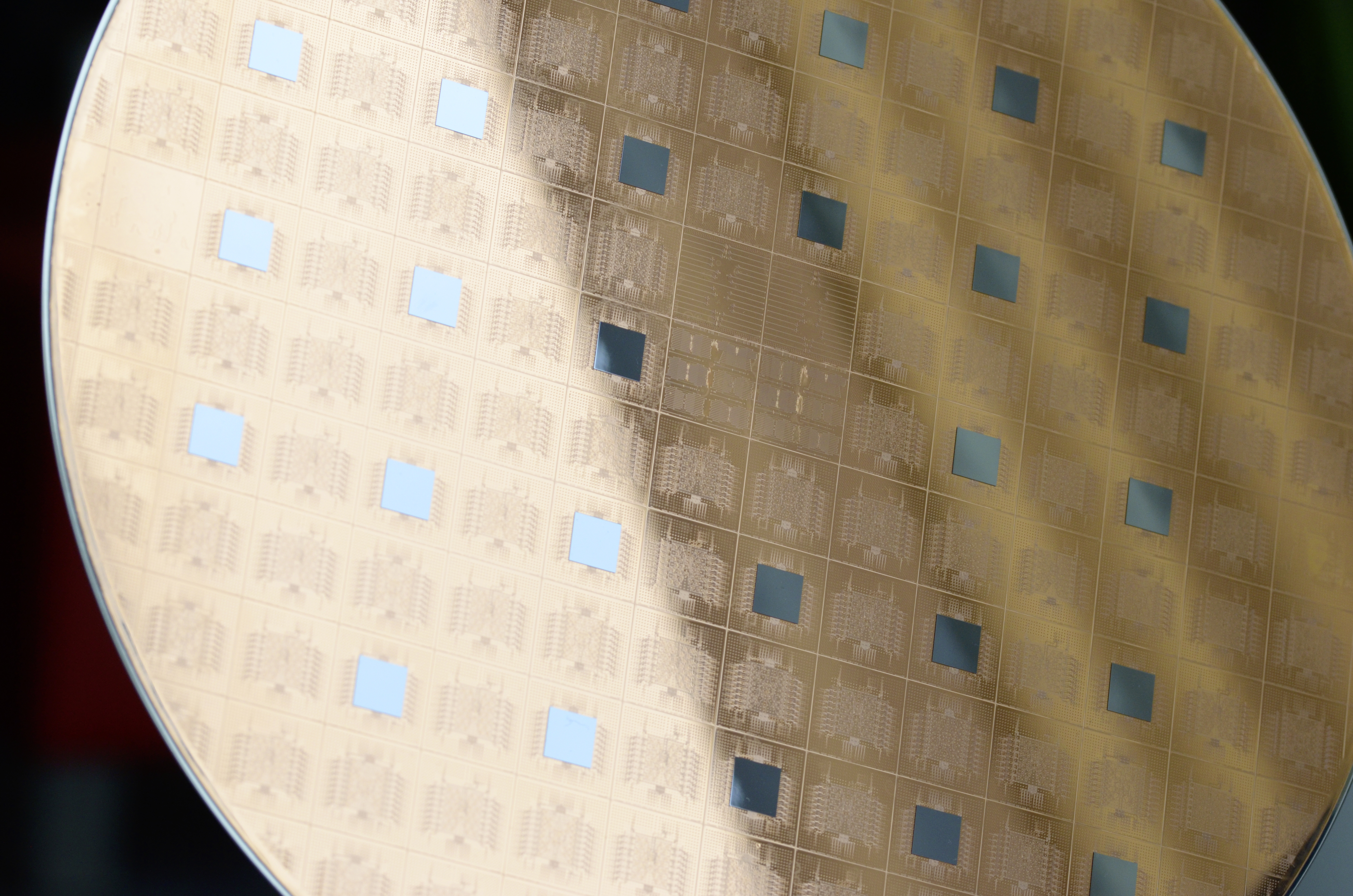
New manufacturing technologies must be developed for the next generation of highly integrated microelectronics. To this end, the European “PIN3S” project is working on processes for the production of ICs with lead spacing of only 3 nm.
These integrated circuits come close to the limits of what is physically possible. They will significantly exceed the performance of today‘s circuits and thus enable applications with particularly high computing power. In autonomous driving, machine learning or in large data centers, they can contribute to leaps in development. In order to reliably produce such structures for high-performance computer chips, innovations are needed in all aspects of manufacturing and the associated measurement technology.
In PIN3S, such novel technologies are brought together and evaluated for the first time in a pilot production line. An additional focus is the further development of the infrastructure for the defect-free production of highly precise masks for wafer production, which serve as templates for the structures to be manufactured.
Fraunhofer IIS / EAS will develop a sensor module for measurement data capturing for wafer exposure with extreme ultraviolet lithography (EUVL).
Last modified: